BeVision M1 Silicon Substrate Surface Cleanliness Analyzer
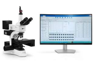
The BeVision M1 static image analyzer provides powerful support for the detection of surface cleanliness of silicon substrate materials
Importance of Surface Cleanliness of Silicon Substrate Materials
In the semiconductor industry, the surface cleanliness of silicon substrate materials is crucial. As the foundation for integrated circuit manufacturing, even tiny contaminants on the surface of silicon substrates can have a serious impact on subsequent processes. An immaculate surface can ensure the smooth progress of key processes such as thin film deposition and lithography and improve the performance and yield of devices. For example, if there are particulate contaminants on the surface, it may lead to short circuits or open circuits in the circuit; organic contaminants may affec the adhesion of the film. Therefore, thoroughly detecting the surface cleanliness of silicon substrate materials is a key link in ensuring the quality of semiconductor products.
Automatic Scanning and Panoramic Stitching
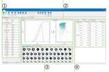
Functions of BeVision M1 Static Image Analyzer The BeVision M1 static image analyzer provides powerful support for the detection of surface cleanliness of silicon substrate materials, greatly saving detection time and labor costs. Equipped with a metallographical microscopy and high-speed CMOS camera, the substrate's surface can be precisely magnified and observed. The BeVision M1 can automatically scan the surface of the substrate, identify and classify defects and impurities based on the size and shape. At the same time, the captured local images can be seamlessly stitched into a full-view image, allowing users to clearly and intuitively observe the surface condition of the entire sample surface.
To avoid being out of focus during scanning, the intelligent auto-focusing function can evaluate the clarity of images in real-time and automatically adjust focus when the clarity
fall below the standard to guarantee the imaging quality. BeVision M1 helps to discover tiny defects (down to 0.3μm) and contaminated areas that may be overlooked, providing a strong guarantee for accurately evaluating surface cleanliness.
| [Measuring principle]: | Static image analysis method, automatically scanning |
| [Parameters]: | Particle size, shape, size and shape distribution, particle count, cleanliness |
| [Measuring range]: | 0.3 – 10,000 μm |
| [Typical measurement time]: | 3 to 10 min * |
| [Scanning range]: | 55 × 55 mm |
| [Functions]: | Scanning mode, panoramic mode, single image analysis, batch images analysis |
| [Microscope]: | Metallographic microscope |
| [Light source]: | Reflective light (Halogen lamp) , transmitted light (Kohler illumination) |
| [Optical lens]: | 4 ×, 5 × BD, 10 × BD, 10 x 20 × (with 40 × digital magnification) ** |
| [Camera]: | CMOS, 12Mpix, up to 120FPS |


